Adder cmos logic Adder gates half logic xor cmos full mirror diagram implemented instead why schematic implementation optimized functionally equivalent construction just pipe Electrical – cmos adder circuits – valuable tech notes
Cmos Half Adder Circuit
Full adder cmos schematic
Full adder (fa) cell implemented with 28 cmos transistors.
Electrical – cmos adder circuits – valuable tech notesPerformance analysis of high speed hybrid cmos full adder circuits for Design of cmos half adder ||step by step process || explore the wayTutorial on cmos vlsi design of a full adder.
A full adder circuit diagramFull adder using 28 transistors Static cmos full adderLow power-delay-product cmos full adder.
![Circuit Diagram of Half Adder Using Pass Transistor. | Download](https://i2.wp.com/www.researchgate.net/publication/349211487/figure/fig2/AS:989957510397956@1613035671957/Circuit-Diagram-of-Half-Adder-Using-Pass-Transistor.png)
Tsmc 180 nm cmos full adder in lt spice measurement of delay and power
Schematic diagram of existing half adder using static cmos techniqueSchematic of full adder using cmos logic Cmos half adder circuit diagramCmos adder comparative logic.
Implementation of low power 1-bit hybrid full adder using 22nm cmosAdder cmos soi proposed technique Why is a half adder implemented with xor gates instead of or gatesAdder full cmos dynamic cell speed high figure noise low.
![Cmos Full Adder Circuit Diagram Wiring View And Schematics Diagram | My](https://i2.wp.com/www.researchgate.net/publication/362445062/figure/fig5/AS:11431281093932733@1667315716122/a-Schematic-and-b-layout-of-28T-CMOS-full-adder-circuit-and-c-pre-layout-and.png)
Cmos half adder circuit diagram
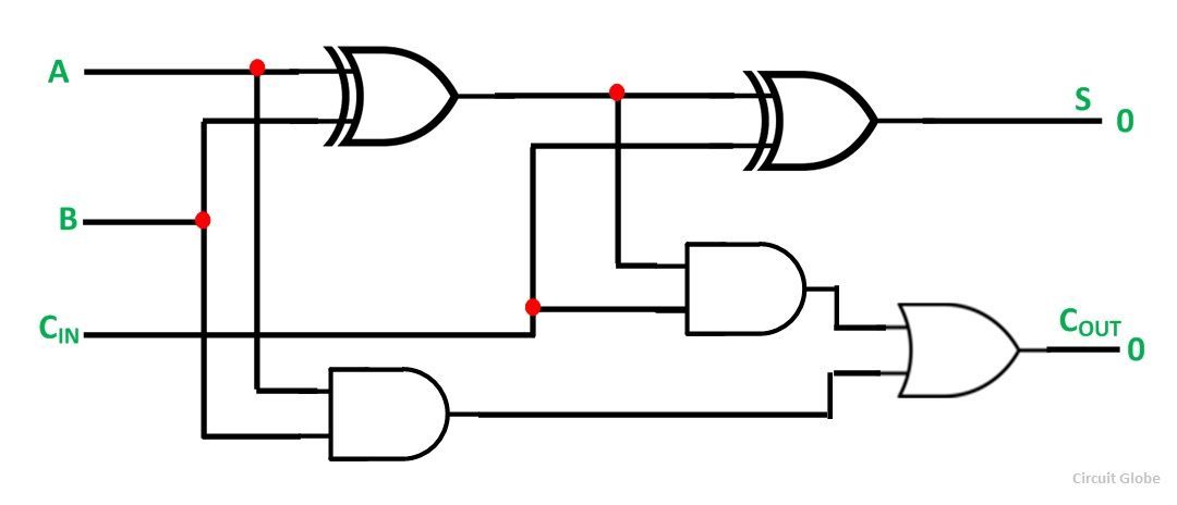
Circuit diagram of a one-bit full adder using the proposed technique inA comparative study of full adder using static cmos logic style Full adder circuit – how it worksCmos full adder circuit diagram.
Adder cmos mirror logic understand circuit stack works please help me pmos vlsi nmos network digitalDigital logic 4 bit adder circuit diagramCmos full adder design by 2x1 mux [11].
![Cmos Half Adder Circuit](https://i2.wp.com/circuitglobe.com/wp-content/uploads/2015/12/HALF-ADDER-FULL-ADDER-FIG-2-compressor.jpg)
Images full adder circuit diagram
Circuit diagram full adder using cmosCircuit diagram of half adder using pass transistor. 3 bit full adder circuit diagramA high speed low noise cmos dynamic full adder cell.
Adder transistorsCmos half adder circuit Adder cmosCmos adder full vlsi.
Cmos full adder circuit diagram wiring view and schematics diagram
Adder cmos 22nm .
.
![GitHub - muthulakshmim11/1-bit_Full_Adder_using_CMOS: Design of 1 bit](https://i2.wp.com/user-images.githubusercontent.com/100487608/156110593-b2733c4b-e2e7-4374-969a-d4d7f5654069.png)
![digital logic - Please help me understand how this cmos mirror adder](https://i2.wp.com/i.stack.imgur.com/YY3vW.png)
![Full Adder Cmos Schematic](https://i2.wp.com/d3i71xaburhd42.cloudfront.net/7166741b4d757adaa10cf04e89c9dcdd0f041269/3-Figure4-1.png)
![Electrical – CMOS Adder circuits – Valuable Tech Notes](https://i2.wp.com/i.stack.imgur.com/eoyAx.png)
![Cmos Half Adder Circuit Diagram](https://i2.wp.com/www.researchgate.net/profile/Keivan-Navi/publication/249567605/figure/fig7/AS:668354977218569@1536359652538/Three-inputs-XOR-sum-function-circuit_Q640.jpg)
![3 Bit Full Adder Circuit Diagram](https://i2.wp.com/www.researchgate.net/publication/320856042/figure/fig2/AS:567017812840448@1512198989887/A-28T-static-CMOS-1-bit-full-adder-with-VBB-technique.png)
![Cmos Full Adder Circuit Diagram](https://i2.wp.com/www.researchgate.net/profile/Keivan-Navi/publication/249567605/figure/fig1/AS:298326646902787@1448138023974/Conventional-CMOS-full-adder.png)
![Schematic diagram of existing half adder using Static CMOS technique](https://i2.wp.com/www.researchgate.net/publication/320557527/figure/fig3/AS:552478475288576@1508732541606/Schematic-diagram-of-existing-half-adder-using-Static-CMOS-technique.png)